LED & Semiconductor
Grish provide polishing products for LED & Semiconductor polishing. We offer both wet and dry polishing suspensions, as well as oil-based and water-based formulations.
OUR STRENGTHS
What Grish Can Do

One-stop Polishing Solutions
GRISH can not only provide you ultra-fine polishing abrasives, we also provide polishing accessories, such as polishing pad, solid wax and dewax liquid which can make your supply chain easier.

Professional Team for Your Service
Our professional Semiconductor material experts are with more than 20 years experiences. We’re honored to help you get the ideal finish that you need.

Cost-effective Process
With an area of more than 12,000m² factory base and reliable manufacture teams, you can be assured of the stability and consistency of our products.
How to Use Grish slurry ?
Application of our Monocrystalline Diamond Slurry in Semiconductor Materials, such as Silicon Carbide Substrate and InP/GaAs Material.
LED & Semiconductor
Polishing Process
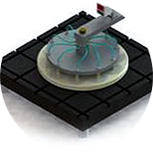
Wax Bonding

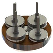
Polishing
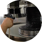
Dewax
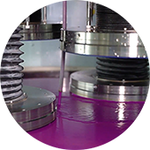
CMP Polishing
InP/GaAs Material Polishing Solution
| InP/GaAs Material Polish Process | Steps | Grish Product |
| Thining (15-30mins) | AO Polish Slurry + Quartz Plate | |
| Back Polishing(30-40mins) | CMP Slurry + Quartz Plate |
GaAs and InP are foundational material for Microelectronics & Photoelectron application, InP as second general of typical Semiconductor material features high light and electron conversion efficiency, great electron mobility, high working temperature and better anti-radiation property, widely applied in optical communication, high frequency MMW, solar energy battery for outer space, etc.
5G network property high frequency & High transmitting speed will need better working performance for RF module, in which InP material will play a critical role. The signal receiver and amplifier made from InP material is able to work on the frequency above 1000GHz with wide broadband and perfect working stability.
Therefore, in 5G era, InP will be a major material for RF module of terminal device and base transceiver station, and the market is booming up.
Grish Newly Polish Process VS Traditional Process
| Silicon Carbide Substrate Traditional Polish Process | Steps | Time |
| Double-sided Lapping (60mins) | ≤11.5h | |
| Precise Lapping (60-90mins) | ||
| Rough Polishing(30-60mins) | ||
| Ultrafine Polishing(240-480mins) |
Grish Newly Silicon Carbide Substrate Polish Process | Steps | Grish Product | Time |
| Double-sided Lapping (30-60mins) | MD Slurry | ≤4h | |
| Rough Polishing(30-60mins) | Nano Diamond Slurry+Rough Polish Pad | ||
| Ultrafine Polishing(120mins) | CMP Slurry + Unique Polishing Pad |
| InP/GaAs Material Polish Process | Steps | Grish Product |
| Thining (15-30mins) | AO Polish Slurry + Quartz Plate | |
| Back Polishing(30-40mins) | CMP Slurry + Quartz Plate |
| Silicon Carbide Substrate Traditional Polish Process | Steps | Time |
| Double-sided Lapping (60mins) | ≤11.5h | |
| Precise Lapping (60-90mins) | ||
| Rough Polishing(30-60mins) | ||
| Ultrafine Polishing(240-480mins) |
|
Grish Newly Silicon Carbide Substrate Polish Process |
Steps | Grish Product | Time |
| Double-sided Lapping (30-60mins) | MD Slurry | ≤4h | |
| Rough Polishing(30-60mins) | Nano Diamond Slurry+Rough Polish Pad | ||
| Ultrafine Polishing(120mins) | CMP Slurry + Unique Polishing Pad |
Explore More In The Video
-
Polishing Solution for Semiconductors